 KOHCTPYKTOP Experimental Sandbox
Welcome, Comrade, to KOHCTPYKTOP: ENGINEER OF THE PEOPLE.
As a design engineer at Semiconductor Factory H3, your job is to construct the circuits described in the design specifications provided to you and have them pass a verification test.
Each circuit has up to eight signals which will be either inputs or outputs. In verification, a series of input signals will be run against your design; to pass the test, the output from your circuit must closely match the expected outputs provided and receive a score of 97% or above.
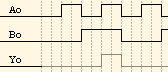 In the left is part of a timing diagram that shows two inputs, A0 and B0, and an output Y0, that was taken from the KT221A DUAL 2-INOUT AND GATE specifications. To pass this verification, Y0 must be high if and only if both A0 and B0 are also high, as shown in the diagram.
In the left is part of a timing diagram that shows two inputs, A0 and B0, and an output Y0, that was taken from the KT221A DUAL 2-INOUT AND GATE specifications. To pass this verification, Y0 must be high if and only if both A0 and B0 are also high, as shown in the diagram.
Circuits are built out of silicon, metal, vias and gates, which are all created by "drawing" them on the circuit grid.
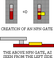
Silicon comes in two variants, N, which is red, and P, which is yellow. Each will conduct signal and can be connected to the metal layer through the use of vias. By drawing a line of one type of silicon and then drawing an overlapping, perpendicular line of the other type you can create a gate; drawing P over N creates an NPN gate (shown left) which will conduct only when the P connection is "hot", while drawing N over P creates a PNP gate that conducts only when the N connection is not "hot".
Metal conducts but is isolated from the silicon layer, connecting to it only at via locations.
A few details about the simulation:
In each cycle of the simulation, values from input signals and dedicated voltage sources (labeled +VCC) are propagated across the entire circuit. Based on whether a gate's activation criterion is met, each gate then stores whether or not is should conduct, a value that is used during the NEXT CYCLE of the simulation.
Thus, activating a gate in one cycle will determine its state in the next, allowing for the construction of stateful and complicated circuits.
This also leads to a real-life phenomenon called "propagation delay", whereby the use of many gates in series leads to lag in parts of the circuit that are down stream, which can cause problems due to de-synchonization of stages.
Custom patterns can consist of a starting pattern and a looping pattern.
In order for the pin to use a custom pattern the pin-type must be any of the 3 in "Custom" group:Patterns are formed with multiple characters commands, generating the expected signal; e.g. 01010 generate a signal with positive logic at 2nd and 4th period.
Non-looping custom patterns will have the last logic assigned at the end; e.g. 01 will generate one negative period at the start and a positive signal infinitelly.
Looping custom patterns can be built with a loop marker (vertical line character), starting pattern is optional; e.g. 00|01 will generate two negative periods at the start and periodic down-up-down-up signal toward infinite.
Any character that doesn't match any code below will be ignored.
This sandbox is based and inspired of the following game:
KOHCTPYKTOP: Engineer of the people by Zachtronics
KOHCTPYKTOP Experimental Sandbox was coded by JustBurner
This work originated from reverse-engineering the original game and trying to make it 100% compatible, plus adding new features over it.
Contents not related to the sandbox such as story and level challenges are not included here but the user can create designs similar to the challenges if so desires.
... also this sandbox (such like the original game) is completely FREE!